JBC Soldering tips C115
JBC Soldering tips
JBC C115 tips are precision-engineered for the NT115 and NP115 Nano handpieces, delivering tip temperatures stabilized to within ±1 °C through JBC's patented Sleep and Hibernation technology. The cartridge design integrates heater and tip in a single replaceable unit, achieving thermal recovery in under 0.5 seconds and operating across a temperature range of 90-450 °C. Tip mass is kept below 1 g, enabling work on 0201 components and fine-pitch SMD pads down to 0.3 mm without thermal overshoot - critical compliance with IPC-A-610 and J-STD-001 rework requirements.
This catalog covers all 32 current C115 cartridge geometries stocked for the NT115 and NP115 Nano series, including conical, chisel, bevel, bent, and micro-tweezers profiles. Each cartridge ships with JBC's iron-plated copper core and is individually tested for resistance continuity and ESD-safe grounding below 2 Ω tip-to-ground, meeting IEC 61340-5-1 requirements for EPA workstation integration.
JBC C115 - Tip series overview for NT115 and NP115
| Tip type | Typical application | Tip width / angle | Key advantage |
|---|---|---|---|
| Conical sharp (C115-C) | Fine-pitch SMD, 0201 pads | 0.3 mm point | Maximum precision, minimal heat spread |
| Chisel (C115-CH) | Through-hole, drag soldering | 0.5-1.0 mm flat | High thermal transfer, fast joints |
| Bevel (C115-B) | QFP, SOIC lead soldering | 30° bevel, 0.8 mm | Large contact area, controlled flow |
| Bent conical (C115-BC) | Recessed pads, BGA inspection | 45° bend, 0.3 mm | Access to hard-to-reach joints |
| Micro-tweezers (C115-TW) | Two-point chip removal, 0402/0201 | Dual 0.3 mm tips | Simultaneous two-pad heating |
| Knife (C115-K) | Wire tacking, flux removal | Blade profile, 1.0 mm | Versatile edge contact geometry |
Typical application areas: PCB rework and hand soldering in electronics manufacturing (IPC-A-610 Class 2/3, J-STD-001), semiconductor packaging and die-attach inspection (SEMI S1/S2), medical device PCB assembly (ISO 13485), automotive electronics repair and prototype assembly (IATF 16949, VDA 6.3), aerospace avionics rework (AS9100), and laboratory / R&D fine-pitch prototyping requiring EPA-compliant ESD-safe tooling (IEC 61340-5-1).
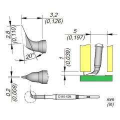
- JBC C115129. Knife-shaped soldering tip, B: 2.8 mm, C115129€59.50Excl. 19% VAT , excl. Shipping Cost
-
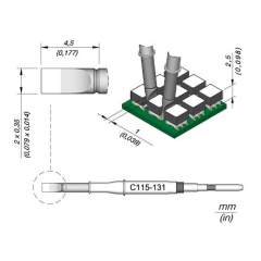
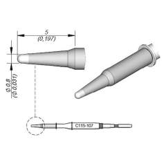
- JBC C115132. Soldering/Desoldering Tip for Nano Soldering Iron NT115€59.50Excl. 19% VAT , excl. Shipping Cost
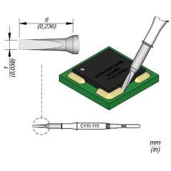
- JBC C115115. Chisel-shaped soldering tip, 6x1 mm, C115115€47.98Excl. 19% VAT , excl. Shipping Cost
-
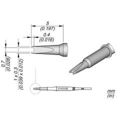
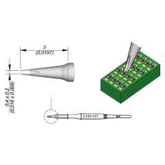
- JBC C115117. Chisel-shaped soldering tip, 0.4x0.2 mm, C115117€39.99Excl. 19% VAT , excl. Shipping Cost
-
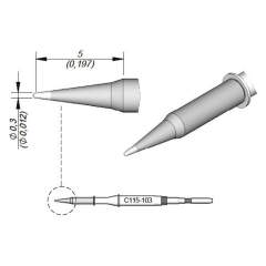
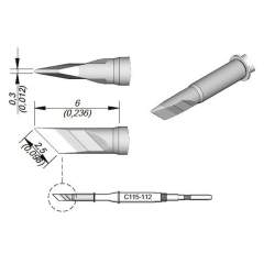
- JBC C115112. Knife-shaped soldering tip, 2.5x0.3 mm, C115112€39.99Excl. 19% VAT , excl. Shipping Cost
-
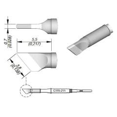
- JBC C115211. Soldering tip blade-shaped, 3.5x0.7 mm, C115211€39.99Excl. 19% VAT , excl. Shipping Cost
-
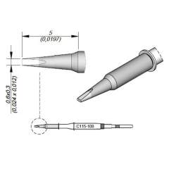
- JBC C115108. Soldering tip chisel-shaped, 0.6x0.3 mm, C115108€39.99Excl. 19% VAT , excl. Shipping Cost
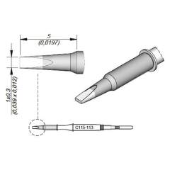
- JBC C115113. Chisel-shaped soldering tip, 1x0.3 mm, C115113€39.99Excl. 19% VAT , excl. Shipping Cost
- JBC C115116. Chisel-shaped soldering tip, 0.2x0.1 mm, C115116€39.99Excl. 19% VAT , excl. Shipping Cost
-
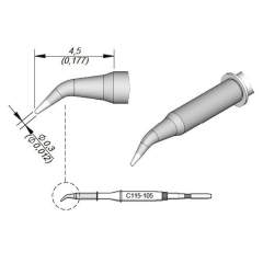
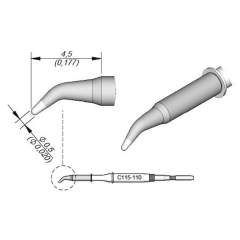
- JBC C115110. Soldering tip conical bent, D: 0.5 mm, C115110€39.99Excl. 19% VAT , excl. Shipping Cost
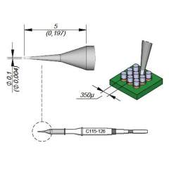
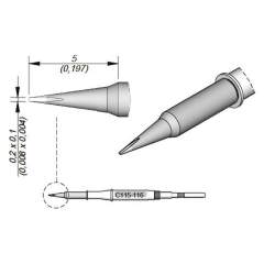
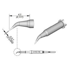
- JBC C115118. Soldering tip conical bent, D: 0.1 mm, C115118€39.99Excl. 19% VAT , excl. Shipping Cost
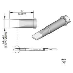
- JBC C115114. Chisel-shaped soldering tip, 1.8x0.5 mm, C115114€39.99Excl. 19% VAT , excl. Shipping Cost
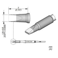
- JBC C115214. Chisel-shaped soldering tip, 1.8x0.5 mm, C115214€39.99Excl. 19% VAT , excl. Shipping Cost
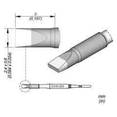
- JBC C115223. Chisel-shaped soldering tip, 2.4x0.6 mm, C115223€39.99Excl. 19% VAT , excl. Shipping Cost