
How do you inspect and grade solder joints to IPC-A-610?
IPC-A-610 is the industry standard for the acceptability of electronic assemblies. A good solder joint is smooth, shiny, shows a concave fillet and full wetting. Joints are graded by eye and microscope against acceptance classes 1, 2 and 3.
To soldering guideHow do you recognise a good solder joint?
IPC-A-610 (Acceptability of Electronic Assemblies) is the most widely used standard for the visual acceptance of solder joints and assemblies. A good joint has a smooth, even surface, a concave fillet between lead and pad, and shows full wetting without torn edges.
Full wetting means the solder spreads flat across pad and lead at a low contact angle instead of balling up on top. The fillet should be concave, that is slightly drawn in. Too much solder hides the contour, too little leaves pad or lead exposed. With lead-free alloys the surface is often duller, which alone is not a defect.
Which solder defects occur most often?
Most solder defects come from too little or too much heat, the wrong amount of solder, or insufficient flux. The table below maps the typical defects to their cause and appearance so they can be spotted reliably during visual inspection.
| Defect | Cause | Appearance |
|---|---|---|
| Cold joint | too little heat, movement while setting | dull, grainy, cracked |
| Too little solder | short solder feed, poor wetting | fillet incomplete, pad exposed |
| Too much solder | solder fed too long | bulbous, contour hidden |
| Bridging (short) | excess solder, tight pitch | solder link between pads |
| Tombstoning | uneven heating, part lifted | chip stood up on one end |
| Voids | trapped gas, outgassing | internal cavity, X-ray only |
| Insufficient wetting | oxidation, little flux | solder balls up, high angle |
| Disturbed joint | movement before solidifying | roughened, warped, dull |
How do you inspect and what do classes 1, 2 and 3 mean?
Inspection starts by eye under good light, adding a stereo microscope at 10x to 20x for fine features and doubtful cases. Internal voids show only under X-ray. IPC-A-610 defines three acceptance classes with rising requirements.
- Class 1 - General electronics: simple products where function is the priority.
- Class 2 - Dedicated service electronics: continued use, longer life, low failure tolerance.
- Class 3 - High-reliability electronics: medical, aerospace and military, where failure is not tolerated.
The class sets how strictly criteria such as minimum wetting, allowed void content or fillet formation are applied. A feature that is acceptable in Class 1 can already be a defect in Class 3. The required class must therefore be fixed before grading begins.
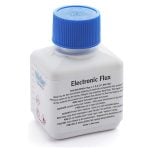 Choose the right flux
The right flux decides wetting and clean fillets that pass visual inspection.
Read flux types guideFrequently asked questions
What is IPC-A-610?
IPC-A-610 (Acceptability of Electronic Assemblies) is the international standard for the visual acceptance of solder joints and electronic assemblies. It defines acceptance criteria and the three classes 1, 2 and 3 with rising reliability requirements.
What does a good solder joint look like?
A good joint is smooth, shows a concave fillet between lead and pad and is fully wetted, meaning the solder spreads out at a low contact angle. With lead-free solder the surface may look duller without being a defect.
What do IPC classes 1, 2 and 3 mean?
Class 1 covers general electronics focused on function, Class 2 covers durable service electronics, and Class 3 covers high-reliability assemblies such as medical or aerospace. The higher the class, the stricter the acceptance criteria.
Solder joint inspection to IPC-A-610 overview
From microscope and lighting to the right soldering equipment, we help you inspect reliably to IPC-A-610.
Per IPC-A-610
Criteria based on a recognised acceptance standard.
Selection help
We help you choose the right products; technical details are clarified with the manufacturer.
Vendor-neutral
Standards and facts instead of product marketing.
Selection help
We help you choose the right products; technical details are clarified with the manufacturer.